Related products

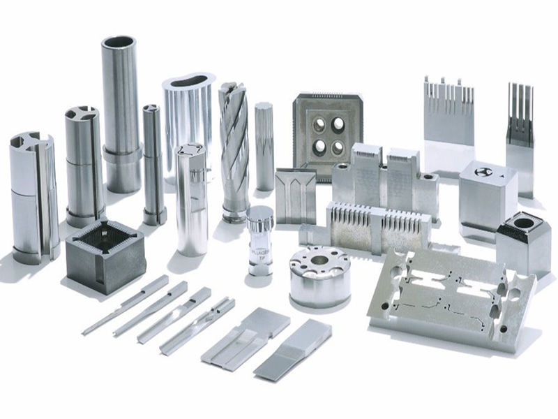
IC Packaging Mold Cavity Bar and Auto Mold Chase
Application: Suitable for TOWA, FICO, ASM, HANMI brand AUTO MOLD SYSTEM
Can be used in conjunction with automatic encapsulation systems to improve the intrinsic quality of the product.Semiconductor Tooling Manufacturer
The semiconductor tooling industry is one of our key markets. We have extensive experience in manufacturing tools for the back-end semiconductor industry, semiconductor packaging, semiconductor leadframes and more. From modules and fixtures for chip attachment to conversion kits for IC test processors to ceramic arms for wafer handling and package and leadframe die components, we have the skills and expertise to build your product to your exacting standards.
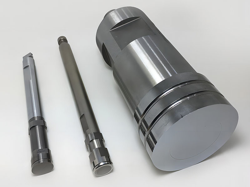
Custom Machining Pot & Plunger for Semiconductor Packaging
The company is one of the largest manufacturers of Pot & Plunger in China and we provide OEM services for Pot & Plunger to well-known semiconductor companies in China and Taiwan.
Pot & Plunger is used in the manufacture of semiconductor packaging moulds. The company's Pot & Plunger can be manufactured using M42 high speed steel or tungsten carbide and can also be supplied with additional PVD coating services.Semiconductor Leadframe Mould & Die Tooling Machining
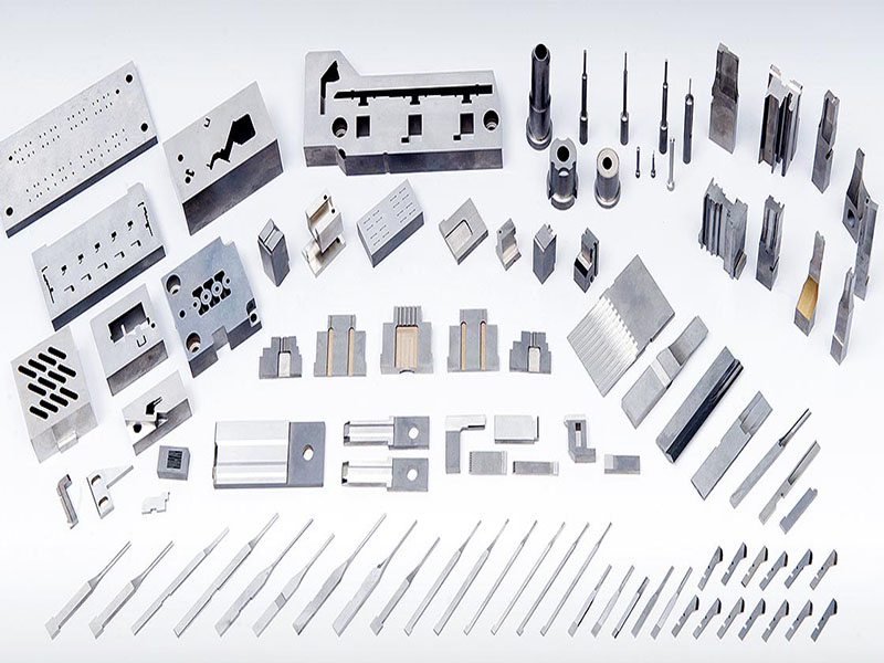
Semiconductor leadframe moulding A metal substrate that serves as a lead to connect a semiconductor chip to external circuitry and as a frame to hold a semiconductor package to a circuit board.
As a key component of a semiconductor integrated circuit, it is connected to the chip by thin leads and transmits electrical signals between the semiconductor chip and the substrate, and acts as a frame to protect and support the chip from external moisture or shocks.